

For this month’s blog, I’m going to provide some useful advice on encapsulation resins to help designers achieve even higher levels of reliability when it comes to protecting circuitry. Potting compounds are increasingly important in the electronics industry where they serve to protect sensitive components from moisture, dust and damage, and help to extend the lifetime of devices. Appreciating the subtle characteristics of resin systems will go a long way in helping you choose the most suitable resin for your application requirements, making the process a lot less complicated and, more importantly, helping you avoid any serious implications for the performance of your application. So, let’s take a closer look at 5 critical factors affecting encapsulation resins, which this month will include potential contaminants, no-clean/cleaning processes, adhesion and best mixing practice.
What potential harm can contaminants wreak if present on a PCB? Can this cause long term problems ultimately resulting in board failure?
There are a number of different contaminants that can cause long-term problems for a PCB. These range from dust and grease to flux residues. Since the resin will stick to the contaminant rather than the board substrate, this produces weak points on the PCB-resin interface, which over time can lead to adhesion failure between the resin and the PCB. Once a fault appears, it can grow in size to allow other contaminants to attack the PCB and components under the resin leading to failure. These contaminants can be chemicals, moisture and/or corrosive atmospheres. In the case of silicone resins, contaminants can prevent the resin from curing properly as the catalysts used in silicone resins are very sensitive.
Why do some applications involve a no-clean process? Is this common within production cycles?
The no-clean process is very common for medium to high volume PCB manufacturing as it takes out the cleaning stages and hence saves time and money. However, it should be noted that no-clean solder and solder pastes usually mean that there is a low amount of flux in the formulation that is left behind. Paradoxically, the flux residues left behind are harder to remove than the traditional systems and adhere well to the PCB substrate.
What are the potential causes and consequences of a lack of adhesion between the resin/PCB/outer casing?
Encapsulation resins are designed to adhere well to a range of substrates varying from FR4 laminate, copper & tinned tracks, the plastics used for components, and the wide range of plastics and metals used for the enclosures/housings. The biggest cause of poor adhesion between a resin and the substrate is dust and/or grease. To gain optimal adhesion, the surface of the substrate should be cleaned to remove any loose debris and to degrease the surface. In the case of plastic housings if they are extruded mouldings the plastic might have a layer of mould release agent on the surface which needs to be removed. If the surface is highly polished, then light abrasion of the surface is often sufficient to improve the adhesion. There are certain plastics that are very hard to get resins to adhere to, polypropylene in particular. It is possible to get surface treated materials, either a silane or plasma pre-treatment, which can help in these cases.
How important is the mixing and dispensing process in the performance of an encapsulation resin?
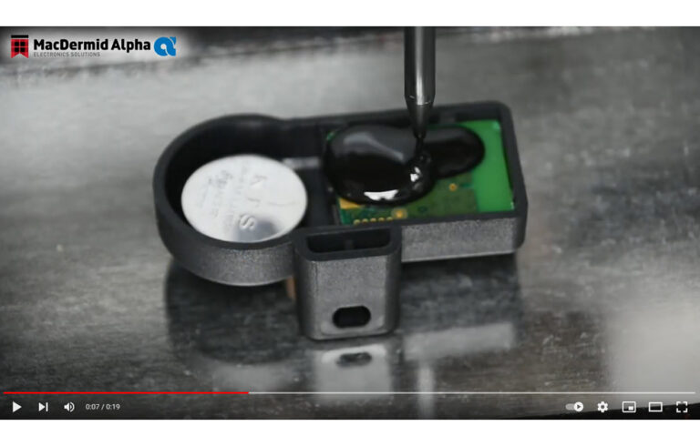
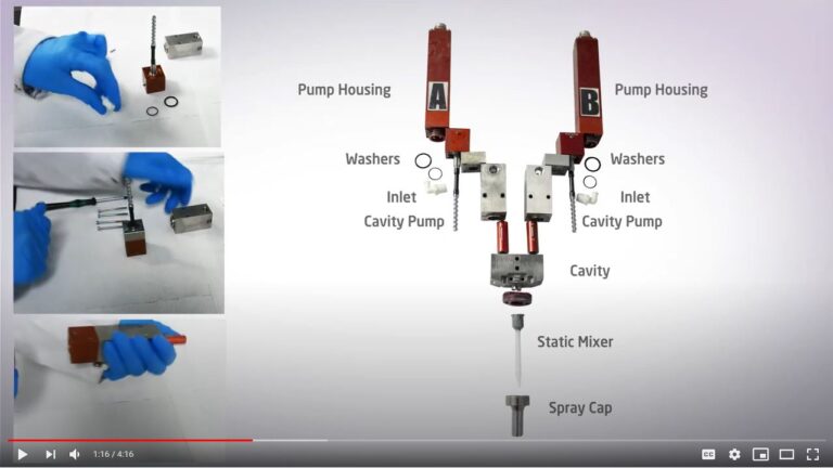
With all 2 component systems mixing is absolutely critical to ensure that the resultant resin performs as described in the TDS. The aim of mixing is to obtain a homogeneous mix with parts A and B distributed uniformly. Incomplete or poor mixing will result at best with a poor performing resin, at worst an uncured resin. Selecting the correct sized static mixer for the machine and resin will enable the resin to be mixed reproducibly with each shot of resin dispensed. Next, the mixed resin has to be placed in the right location to allow it to flow across the PCB, displacing air from any voids and to coat the components to the required thickness. Air trapped in the resin is another source of potential weakness within the resin as this can lead to a physical weakness due to thermal cycling, physical shock, chemical ingress, or in the case of high voltages, a concentration point where corona can build up.
Walk me through your top tips for the manual mixing process of a resin pack.
Firstly, select the right size resin pack for the job. If a lot of small volume units are to be potted, it might be easier to use a couple of small resin packs than a single large one, to allow more time to dispense the material accurately and the useable life/pot life of a small volume of resin is usually longer than with a large volume.
In the case of polyurethane and silicone resins, make sure that the foil pack is sealed before use. Do not open the outer packs until ready to mix and dispense.
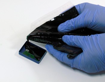
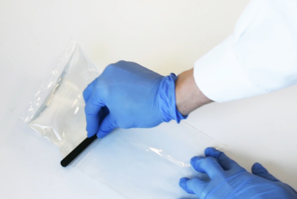
Remove the resin pack from the outer packaging and remove the middle clip separating the two halves of the pack. Use the clip to push the resin from one half of the pack into the other. Take the resin pack in the hand and mix for a couple of minutes.
Lay the pack on a flat surface and, using the clip, push the material into the centre of the pack. Pay particular attention to the corners. Continue mixing vigorously for another couple of minutes.
On a flat surface use the clip to push the mixed material into the half of the pack with the angled seal. Roll up the other end of the pack to the bottom edge of the mixed resin.
Cut the corner of the pack off and slowly decant the resin over the PCB or into the enclosure. Allow the resin to flow so that any air under or between components or wiring can be displaced. For complicated geometries it might be better to add the required amount of resin in multiple stages to allow the air to be released, control the exotherm experienced by the components and to obtain the desired thickness.
If adding a second layer of resin, wait until the first layer has gelled before adding the second.
If in any doubt, it is always advisable to discuss with suppliers which type of resin system is most appropriate for your application. The technical support teams of reputable suppliers have a wealth of experience to call upon and, should it become necessary, they have the expertise to modify chemical formulations in order to meet your particular application needs. I hope the points covered this month have been informative and please do look out for my next blog, where I’ll be covering more issues on getting the most out of encapsulation resins for seamless circuit protection. In the meantime, please do get in contact if you have any questions you would like to ask.